English 简体中文
Service
PCB Fabrication
Your current position:Home > Service > PCB Fabrication


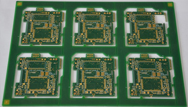
PCB fabrication, also known as PCB manufacturing, is the process of producing printed circuit boards (PCBs) that serve as the foundation for electronic devices. The fabrication process involves several steps to transform a design concept into a physical PCB. Here's an overview of the PCB fabrication process:

  1. Design Input:

    • The process begins with the input of the PCB design files, typically in Gerber format, which include information about the layout, copper traces, and other essential elements of the PCB.
  2. Panelization:

    • Multiple PCBs are often combined into a panel for more efficient manufacturing. This step involves arranging individual PCBs on a larger panel, allowing for simultaneous fabrication of multiple boards.
  3. Substrate Preparation:

    • The base material, known as the substrate or core, is prepared. Common substrate materials include fiberglass-reinforced epoxy laminates (FR-4). The substrate is typically coated with a thin layer of copper on both sides.
  4. Copper Cladding:

    • Copper foil is laminated onto the substrate using heat and pressure. The thickness of the copper layer is determined by the specific requirements of the PCB design.
  5. Photoresist Application:

    • A layer of photoresist is applied to both sides of the copper-clad substrate. Photoresist is a light-sensitive material that will be used to define the traces and features of the PCB.
  6. Exposure and Development:

    • The PCB design is transferred onto the photoresist using a process called exposure. UV light is used to expose the photoresist through a mask that contains the PCB design. After exposure, the unexposed areas are washed away during the development process.
  7. Etching:

    • The exposed copper is etched away using a chemical solution. The remaining copper forms the conductive traces of the PCB. The etching process ensures that only the desired copper areas defined by the design remain on the board.
  8. Layer Alignment and Bonding (for Multilayer PCBs):

    • In the case of multilayer PCBs, individual layers are aligned and bonded together. This may involve using heat and pressure to ensure a secure bond between layers.
  9. Drilling:

    • Holes are drilled into the PCB for component mounting and interconnection. The locations and sizes of these holes are specified in the design files.
  10. Through-Hole Plating (if applicable):

    • For plated-through holes, a thin layer of conductive material is plated onto the hole walls to create an electrical connection between different layers.
  11. Solder Mask Application:

    • Solder mask is applied over the copper traces to protect them from oxidation and to define areas where components will be soldered. This step also helps prevent unintended short circuits.
  12. Silkscreen Printing:

    • Information such as component outlines, reference designators, and other markings are printed on the PCB using a silkscreen ink.
  13. Surface Finish (if applicable):

    • The final surface finish is applied to protect the exposed copper and enhance solderability. Common surface finishes include HASL (Hot Air Solder Leveling), ENIG (Electroless Nickel Immersion Gold), and OSP (Organic Solderability Preservatives).
  14. Testing:

    • The fabricated PCBs undergo testing to ensure that they meet the design specifications. Testing may include checks for electrical continuity, shorts, and other parameters.
  15. Final Inspection:

    • A final inspection is conducted to verify that the PCBs meet quality standards. This may involve visual inspection and measurements.
  16. Packaging and Shipping:

    • The finished PCBs are packaged and prepared for shipping to the end-user, where they will be assembled into electronic devices.

The entire PCB fabrication process involves a combination of precision machinery, chemical processes, and quality control measures to produce reliable and functional PCBs for use in electronic products. Advanced technologies and automation play a significant role in achieving high precision and efficiency during PCB fabrication.


About Us
Company Profile
Links
Global Sources
Linkedin
Twitter
Facebook
News
Industry News
Company News
Products
PCB Fabrication
PCB design services
PCB Assembly
Components Procurement
Manufacturing Capability
Function Testing
    sales@japcbpcba.com                   Monday - Sunday : 9:00 - 22:00                  Copyright © JA Electronics Co.,Limited