PCB design, or printed circuit board design, is the process of creating the layout for the components and connections on a PCB. PCBs are crucial in the functioning of electronic devices, providing a platform for connecting and supporting electronic components. Here's an overview of the PCB design process:
-
Schematic Design:
-
The process usually begins with the creation of a schematic diagram that outlines the connections between different electronic components. This is a graphical representation of the circuit's structure.
-
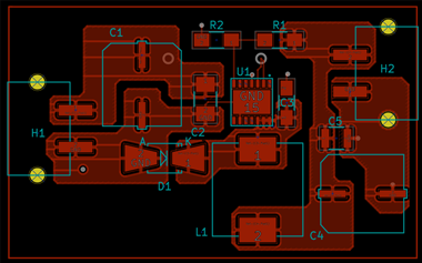
Component Placement:
-
Once the schematic is complete, the next step is to place the components on the PCB layout. The goal is to arrange them in a way that minimizes signal interference, ensures proper heat dissipation, and allows for efficient routing.
-
Routing:
-
Routing involves creating pathways or traces that connect the various components on the PCB. Careful attention is given to the arrangement to optimize signal integrity and reduce electromagnetic interference (EMI). Traces must also consider factors like impedance matching and signal integrity.
-
Ground and Power Planes:
-
Designers often include ground and power planes on the PCB. Ground planes help in reducing noise and providing a stable reference point for signals, while power planes distribute power throughout the board efficiently.
-
Design Rules Check (DRC):
-
After completing the layout, designers run a Design Rules Check to ensure that the design meets manufacturing requirements and standards. This includes checking for proper clearances, trace widths, and other specifications.
-
Gerber Files Generation:
-
Gerber files are the standard file format used in PCB manufacturing. These files contain the information necessary for creating the different layers of the PCB. Designers generate Gerber files for fabrication.
-
Prototype and Testing:
-
Before mass production, it's common to create a prototype of the PCB. This allows designers to test the functionality and identify any issues that may arise during manufacturing or in the final product.
-
Manufacturing:
-
Once the design is finalized and validated, the PCB design files are sent to a manufacturer for mass production. The manufacturer follows the specifications provided in the Gerber files to produce the actual PCBs.
-
Assembly:
-
After manufacturing, electronic components are soldered onto the PCB through a process called PCB assembly. This can be done manually for prototypes or using automated assembly lines for large-scale production.
-
Testing and Quality Control:
-
The final step involves testing the assembled PCBs to ensure they meet quality standards and function correctly. This may involve various tests, including functional testing, electrical testing, and sometimes environmental testing.
PCB design is a critical aspect of electronic product development, influencing factors such as performance, reliability, and manufacturability. Advanced PCB design tools and simulation software are often used to optimize designs before prototyping and production.
 sales@japcbpcba.com
  Monday - Sunday : 9:00 - 22:00 Copyright © JA Electronics Co.,Limited